
A recent comprehensive analysis has brought into sharp focus the escalating challenge of managing per- and polyfluoroalkyl substances (PFAS) waste originating from the global semiconductor manufacturing industry. Driven by the surging demand for advanced electronics and the transformative power of generative AI technologies, this sector is on a trajectory of unprecedented growth, yet it simultaneously confronts a formidable environmental obstacle in the form of pervasive PFAS contamination. The research, which synthesizes insights from a pivotal workshop, establishes a clear consensus among experts from academia, industry, and government, outlining the current state of science and policy while proposing a strategic and essential roadmap toward a more sustainable future.
The Scope of the Crisis
The ‘Forever Chemical’ Dilemma
The central issue stems from the unique and paradoxical chemical properties of PFAS, often referred to as “forever chemicals” for their extreme persistence. These substances are indispensable in critical semiconductor manufacturing processes, including high-precision photolithography and etching, where their unparalleled stability and performance are vital for creating microscopic circuits. However, this same chemical resilience that makes them so valuable in production also renders them extraordinarily difficult to break down in the environment. This persistence leads to widespread and long-lasting contamination of soil, water, and ecosystems, posing significant health risks to both human populations and wildlife. As regulatory frameworks across the globe become increasingly stringent and public awareness of the inherent dangers of PFAS grows, the semiconductor industry faces mounting pressure to innovate and adopt sustainable waste management practices that can effectively mitigate these profound environmental liabilities without impeding critical technological progress.
The Challenge of Complex Industrial Waste
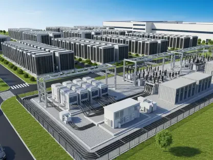
The sheer scale of the waste management problem confronting the semiconductor industry presents a formidable challenge that cannot be understated. A single large-scale semiconductor fabrication plant, or “fab,” can generate thousands of cubic meters of wastewater on a daily basis. This effluent is far from simple; it is an intricate and highly complex “soup” of industrial byproducts that defies easy treatment. This mixture contains a diverse and shifting array of PFAS compounds, along with a host of other contaminants, including various solvents, heavy metals, and salts, which significantly complicates any and all remediation efforts. The inherent complexity of this industrial waste stream renders many conventional water treatment methods, which are typically designed for less concentrated or simpler waste profiles, almost completely ineffective. This reality underscores the urgent and non-negotiable necessity for the development of innovative and specialized solutions that are specifically engineered to address this unique and challenging contamination profile.
Pathways to Mitigation and Their Hurdles
A Three-Pronged Strategy: Monitor, Separate, Destroy
In response to this pressing environmental need, a consensus is forming around a multi-faceted strategy for effective PFAS mitigation that prioritizes three critical focus areas: improved monitoring, efficient separation, and safe destruction. For monitoring, the emergence of advanced analytical tools represents a promising new frontier. The strategic integration of artificial intelligence with high-resolution mass spectrometry, for example, offers a powerful and precise method for accurately tracing the origins of different PFAS compounds. This allows for a deeper understanding of their chemical transformations as they move through the intricate manufacturing and waste treatment processes. On the destruction front, research is highlighting technologies specifically designed to break the exceptionally strong carbon-fluorine bonds that define PFAS molecules. Advanced methods such as plasma discharge and electrochemical oxidation represent significant advancements toward developing robust, reliable, and scalable treatment systems capable of permanently neutralizing these hazardous chemicals.
Technical Barriers: Adapting Technology for Industrial Scale
Despite these promising technological advancements, several substantial hurdles stand in the way of their practical and widespread implementation across the industry. A primary issue is that many existing PFAS treatment technologies were not developed with industrial applications in mind; they were initially engineered for municipal water systems, which must contend with far lower concentrations and significantly less complex chemical matrices than industrial wastewater. As a result, these systems often fail to adequately address the specific types of PFAS that are prevalent in semiconductor production, particularly the short and ultrashort-chain variants, which are notoriously difficult to capture and treat using conventional methods. Consequently, a significant and concerted research and development effort is now required to adapt, re-engineer, and optimize these technologies to effectively manage the high-strength, chemically complex industrial waste streams characteristic of modern semiconductor fabrication.
Logistical Nightmares: Integrating Solutions into Existing Facilities
Integrating any new waste treatment solution into an operational semiconductor fabrication facility presents a monumental logistical challenge that extends far beyond the technology itself. A typical semiconductor fab is a highly optimized, multi-billion-dollar operation where every single step is meticulously controlled and interconnected. Such a facility could easily have hundreds or even a thousand distinct manufacturing steps, all of which are integrated with one another in a delicate, high-precision dance. Any new system, therefore, must be seamlessly incorporated into this existing and highly tuned operational framework without causing any disruption to the delicate manufacturing processes. This requires not only that the new technology be effective at removing PFAS from the waste stream but also that it can be implemented within the physical and operational constraints of a facility that was not designed to accommodate it, making retrofitting a complex and costly endeavor.
Building a Sustainable Future
Beyond Technology: Scientific and Regulatory Frontiers
Beyond the immediate technical and engineering challenges, the path to successful PFAS mitigation is paved with several critical non-technical factors that are paramount for long-term success. A deeper and more nuanced scientific understanding of the transmutable chemical properties of PFAS is essential. These substances can change their chemical form during both manufacturing and treatment processes, potentially creating new, unregulated byproducts with unknown environmental impacts. Additionally, the industry must move beyond a reactive stance and proactively anticipate forthcoming regulatory measures to ensure long-term compliance and avoid future liabilities. For researchers in the field, two key barriers continue to impede progress: a significant lack of access to real industrial waste streams for the experimental validation of new technologies, and the considerable challenge of scaling up promising laboratory-developed solutions for practical, cost-effective implementation in large-scale industrial settings.
A Call for Collaboration: Uniting Academia, Industry, and Policy
A central and recurring theme emerging from the analysis is the urgent and non-negotiable call for enhanced collaboration among academia, industry, and policymakers. Building robust and functional partnerships between these key stakeholders is absolutely essential for developing the integrated, holistic solutions needed to achieve a “zero-discharge” future for semiconductor manufacturing. This ambitious vision requires the creation of compact, cost-effective, and highly efficient treatment systems that can function effectively within the significant space and resource constraints of both existing and future factories. The expert consensus serves as a rallying cry for collective action, presenting a compelling and data-driven case for proactive engagement and a sense of shared responsibility in addressing the PFAS waste crisis. The complexity of the problem demands a unified approach, as no single entity can solve it alone.
The New Paradigm: Environmental Stewardship as a Prerequisite for Growth
The comprehensive analysis of PFAS waste management in semiconductor manufacturing ultimately underscored the intricate and deeply intertwined relationship between technological advancement, environmental stewardship, and regulatory policy. The roadmap outlined by researchers reflected a growing recognition across sectors that sustainable practices were not an impediment to economic growth but rather a fundamental prerequisite for it in the modern era. By fostering a culture of interdisciplinary collaboration and committing to sustained innovation, the semiconductor industry positioned itself to successfully navigate the complex challenges of PFAS management. The continued research, open dialogue, and collective action of all stakeholders became pivotal in shaping a future where this vital industry could thrive in harmony with environmental safety, ensuring a healthier and more sustainable world was possible for generations to come.