
The pursuit of ultra-efficient energy generation has entered a transformative phase as researchers successfully demonstrate solar cell architectures capable of converting more than one-third of the sun’s incident light into usable electricity. This milestone represents a departure from decades of incremental gains in traditional silicon technology, which has long hovered near its theoretical physical limits. By layering different semiconductor materials to capture a broader spectrum of solar radiation, scientists have effectively bypassed the constraints of single-junction devices. This shift not only promises to lower the cost of renewable energy but also fundamentally redefines the feasibility of high-density urban power generation where space is at a premium. As global demand for clean energy intensifies, these high-efficiency cells serve as a critical bridge toward a sustainable future, ensuring that the next generation of power infrastructure is both more compact and productive.
Surpassing Silicon Efficiency Limits
The Science: Multi-Junction Absorption
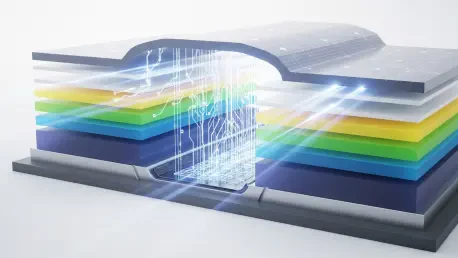
The fundamental limitation of standard silicon solar cells lies in their inability to efficiently process high-energy photons from the blue end of the light spectrum. While silicon is an excellent absorber of near-infrared light, higher-energy light often loses its excess energy as heat before it can be converted into electrical current. To solve this, researchers have developed tandem structures that place a wide-bandgap material, typically a perovskite semiconductor, directly on top of a narrow-bandgap silicon base. The top layer absorbs the high-energy blue and green light, while the bottom silicon layer captures the lower-energy red and infrared rays. This dual-layered approach creates a more comprehensive utilization of the solar spectrum, allowing the device to exceed the 29.4 percent theoretical maximum efficiency established for single-junction silicon units. By optimizing the bandgap of the perovskite layer, engineers have achieved a record-breaking 33 percent efficiency.
Material Synergy: Optimizing the Interface
Achieving such high efficiency requires precise control over the refractive indices and electrical connectivity between the layered materials. One of the primary engineering challenges involves the development of recombination layers that facilitate the movement of charge carriers between the perovskite and silicon without significant resistance. Advanced deposition techniques, such as vacuum evaporation and multi-step solution processing, are utilized to ensure that the perovskite film is uniform and free of microscopic defects that could trap electrons. Moreover, the texturing of the silicon surface, which is traditionally used to reduce light reflection, must be carefully balanced with the need for a flat foundation for the perovskite layer. Solving these optical and electrical hurdles has required deep interdisciplinary collaboration across materials science and chemistry. The resulting devices demonstrate that the synergy of materials can overcome the intrinsic properties of any single substance.
The Path Toward Commercial Scale
Stability: Shielding the Active Layers
Despite the impressive efficiency gains observed in the lab, the transition from experimental prototypes to mass-produced panels necessitates overcoming significant hurdles related to environmental stability. Perovskite materials are historically sensitive to moisture and heat, which can cause them to degrade much faster than silicon components. To address this, manufacturers are implementing sophisticated encapsulation techniques that shield the active layers from the atmosphere. Advanced barrier films and edge seals are being tested to ensure these panels can withstand twenty-five years of outdoor exposure, matching the current industry standard for silicon reliability. Researchers are also exploring the replacement of volatile organic components within the perovskite crystal structure with more stable inorganic alternatives. These modifications aim to enhance the thermal stability of the cells, ensuring they maintain peak performance through the 2026 to 2028 deployment cycle.
Economics: Scaling for Global Demand
The industry moved toward a hybrid manufacturing model that prioritized both performance and resilience in the face of changing climate patterns. Investors recognized that the jump to thirty-three percent efficiency was not merely a scientific achievement but a necessary evolution to keep pace with the rising global demand for localized power generation. Project managers implemented strict quality control protocols that accounted for the specific degradation pathways of multi-junction devices, ensuring that early installations provided consistent data for future iterations. Grid operators also adjusted long-term planning to accommodate the higher energy density provided by these modules. By diversifying the supply chain and investing in domestic manufacturing capabilities for perovskite materials, stakeholders mitigated the risks associated with raw material scarcity. These actions established a robust framework for integrating high-efficiency solar into the national grid.